Parasitic Capacitance
Parasitic capacitance (also called stray capacitance) is an unintended capacitance that occurs between parts of an electronic component or circuit due to their proximity to each other.
It is not designed as part of the circuit, but it exists due to the physical layout and material properties of the components.
Basic Capacitance Principle:
Capacitor is a device that stores electrical energy by accumulating electric charges on two closely spaced surfaces that are insulated from each other.
C = ε.A/d
- C = Capacitance (F)
- ε = Permittivity of the dielectric
- A = Area of overlapping conductors
- d = Distance between them
Even when we don’t intend to create a capacitor, this physical reality applies. Hence, stray or parasitic capacitance arises in real-world circuits.
Why Does Parasitic Capacitance Exist?
Any two conductive elements separated by an insulator (dielectric) have the ability to store electric charge, forming a capacitor — even if unintentionally. In high-speed or high-frequency circuits, these effects become non-negligible.
Causes of Parasitic Capacitance
- PCB Traces Close Together
- Long and parallel traces on a PCB can create capacitive coupling.
- Long and parallel traces on a PCB can create capacitive coupling.
- Adjacent Components
- Pins on an IC package or connector can have inter-pin capacitance.
- Pins on an IC package or connector can have inter-pin capacitance.
- Component Leads & Sockets
- Leads and socket connectors can act like capacitive plates.
- Leads and socket connectors can act like capacitive plates.
- Multilayer PCBs
- Power and ground planes separated by a dielectric form capacitors.
- Power and ground planes separated by a dielectric form capacitors.
- Cables
- Coaxial or twisted-pair cables can have parasitic capacitance between conductors.
- Coaxial or twisted-pair cables can have parasitic capacitance between conductors.
Example 1: Parasitic Capacitance in a PCB Trace
Two traces running side-by-side for 10 cm can exhibit a parasitic capacitance of a few picofarads (pF). At high frequencies, this could lead to signal distortion or crosstalk.
Example 2: MOSFET Gate Capacitance
In a switching circuit, the drain-gate parasitic capacitance in a MOSFET can slow down switching transitions, increasing power loss.
Parasitic Capacitance effect on Circuits
A. In Analog Circuits:
- Low-pass Filtering: Parasitic capacitance with signal resistance forms RC filters → bandwidth loss.
- Miller Effect: In amplifiers, feedback capacitance is amplified, reducing bandwidth.
B. In Digital Circuits:
- Rise/Fall Time Degradation: Extra capacitance loads the driver, causing slow edges.
- Crosstalk: Capacitive coupling allows signal energy to “leak” between traces.
- Timing Skew: Delays in signal transitions due to unequal parasitic loading.
C. In Power Electronics:
- Switching Losses: MOSFET drain-gate capacitance increases transition energy.
- EMI Emission: Fast switching of capacitively coupled nodes causes high-frequency noise.
Disadvantages of Parasitic Capacitance
1. Performance Limitations
- Slower signal transitions.
- Limits max operating frequency in high-speed designs.
2. Signal Integrity Issues
- Causes waveform distortion, rise/fall time degradation
- Overshoot, ringing, and degraded eye diagrams in digital interfaces.
3. Power Loss
- Each switch charge/discharge cycle consumes energy:
E = 1/2CV2
4. Amplifier Instability
- Phase shift due to capacitance can cause oscillations.
Amplifiers may become unstable due to unintentional feedback paths.
5. Increased EMI
- Capacitively coupled paths can radiate or pick up noise.
Role of Parasitic Capacitance in EMI/EMC
A. EMI (Electromagnetic Interference)
- Stray Capacitance forms coupling paths for high-frequency signals.
- Unshielded traces with parasitic Capacitance can radiate energy like dipole antennas.
B. EMC (Electromagnetic Compatibility)
- Parasitic C makes circuits vulnerable to external RF fields.
- Inter-device capacitance (e.g., between chassis and ground) can allow conducted interference.
Example: Power Converter EMI
In a buck converter, the drain of a MOSFET has high dV/dt. Parasitic capacitance between the drain and heatsink or ground can cause common-mode EMI, leading to EMC test failures.
Mitigation Techniques & Solutions
A. PCB Design Techniques
- Trace Separation: Increase distance between high-speed or sensitive lines.
- Minimize Overlap: Avoid overlapping high-speed traces on adjacent layers.
- Use Ground Planes: Acts as a reference and return path, reduces loop area.
- Short Trace Lengths: Shorter paths reduce distributed parasitic capacitance.
B. Component Placement
- Place analog and digital parts separately.
- Keep high-impedance nodes away from switching signals.
C. Guard Rings & Shielding
- Grounded copper around sensitive analog lines to absorb capacitive noise.
- Use shielded cables or enclosures where needed.
D. Termination Techniques
- Use proper series or parallel termination to match impedance and reduce reflections.
- Helps prevent additional capacitive loading effects.
E. Differential Signaling
- Common in LVDS, USB, Ethernet.
- Rejects common-mode noise from capacitive coupling.
F. Simulation and Modeling
- Use tools like LTspice, Altium, Ansys HFSS to simulate parasitic behavior.
- Extract layout parasitics and optimize during design.


Common-Mode vs. Differential-Mode Noise
Electrical Noise
Electrical noise is any unwanted signal superimposed on a desired electrical signal that can distort, interfere, or reduce signal fidelity. In high-speed circuits and EMC analysis, this noise is typically classified as:
-
Differential-Mode (DM) Noise
-
Common-Mode (CM) Noise
These two have different origins, transmission paths, and countermeasures.

1. Differential-Mode Noise – “Normal-mode noise”
Differential-mode noise is the voltage difference between two conductors of a signal or power line. It represents the intentional signal path where the noise rides in opposition across the two conductors.
Current Flow:
The noise flows in opposite directions in a loop between the two wires. If one conductor has a +5V spike and the other has -5V, the differential noise is 10V.
Example Use Cases:
-
Power rails: +V and GND in DC systems
-
Communication: USB, HDMI, Ethernet pairs
-
Analog signals: Sensor lines in instrumentation
Typical Sources:
-
Switch-mode power supplies (SMPS) – due to rapid switching
-
High-speed data lines – signal reflections, ringing
-
Magnetic coupling – between traces or cables
-
Load changes – from motors, solenoids, or relays
Mitigation Strategies:
-
Differential-mode filters: Series inductors with capacitors across lines
-
Matched impedance design: Prevents signal reflection and ringing
-
Twisted pairs: Cables twisted to cancel out opposing fields
-
Short trace lengths: Reduces antenna effect
2. Common-Mode Noise – “Ground-referenced noise”
Common-mode noise appears equally and in phase on both conductors relative to a common reference point, usually system ground or chassis.
Current Flow:
Both wires carry the noise in the same direction, and the return path flows through the ground plane, earth, or shielding.
Real-World Example:
-
Long USB cables pick up RF noise equally on both data lines.
-
AC power lines exposed to EMI from nearby radio towers or industrial machines.
Typical Sources:
-
Electrostatic coupling: From nearby high-voltage lines
-
Radiated emissions: Antenna-like behavior of cables or traces
-
Ground potential differences: Between system components (e.g., USB ground loop)
-
Parasitic capacitance: Between PCB traces and the chassis
Mitigation Strategies:
-
Common-mode chokes: High impedance to CM signals, low to DM signals
-
Shielded cables and connectors: With 360° termination to chassis
-
Isolated grounds: Breaks in ground loops
-
Ferrite beads/clamps: On external cables
3. Visualizing the Current Paths
Noise Type: Differential Mode
Current Direction: Opposite directions on each line, Reference Point: Across the pair, Return Path: One conductor to another
Noise Type: Common Mode
Current Direction: Same direction on both lines, Reference Point: Ground or chassis, Return Path: Through system or earth ground

4. Importance in EMC Testing
Emissions:
-
Differential-mode emissions are mostly conducted (via power/signal lines).
-
Common-mode emissions often become radiated, as CM currents form large loop areas (acting like antennas).
Compliance Implications:
-
Regulatory bodies (e.g., FCC, CISPR, IEC) test both emission types.
-
CISPR 22/32 and FCC Part 15 focus heavily on common-mode conducted emissions in lower frequency bands (150 kHz–30 MHz).
5. Filtering Techniques Comparison
Filter Type: CM Filter
Effective Against: Common-mode noise, Components Used: Common-mode choke, Y-capacitors
Filter Type: DM Filter
Effective Against: Differential-mode noise, Components Used: Series inductors, X-capacitors
Notes:
-
Y-capacitors connect from line to ground (handle CM).
-
X-capacitors go across the line pair (handle DM).
6. Example: SMPS Input Filtering
In a switch-mode power supply, both noise types are generated:
-
Differential noise arises from the switching node oscillations.
-
Common-mode noise results from parasitic capacitance between high-frequency switching nodes and the chassis.
The input filter typically includes:
-
X-capacitor across line and neutral (DM)
-
Y-capacitors from line/neutral to ground (CM)
-
Common-mode choke for both conductors
7. Application-Specific Impacts
High-Speed Digital Systems:
-
Differential signaling (LVDS, HDMI, USB) relies on clean DM paths. Noise degrades data integrity (eye diagrams, jitter).
-
CM noise can cause cross-talk between pairs or fail EMC radiated tests.
Automotive:
-
CM noise is a major concern due to long wire harnesses acting as antennas.
-
Standards like ISO 11452 and CISPR 25 require thorough CM filtering.
Medical Devices:
-
Safety and immunity to external EMI are critical—isolation transformers, CM chokes, and filtering are used to ensure patient safety and compliance (e.g., IEC 60601-1-2).
Conclusion
|
Aspect |
Differential-Mode Noise |
Common-Mode Noise |
| Flow Direction | Opposite on conductors | Same on both conductors |
| Reference | Between lines | Against ground or chassis |
| Typical Source | Internal circuit switching | External EMI, parasitic coupling |
| Testing Concern | Conducted emissions | Radiated + conducted emissions |
| Mitigation | X-caps, twisted pairs, impedance match | CM chokes, Y-caps, shielding |
Both types of noise must be addressed for:
-
Regulatory compliance
-
Signal integrity
-
Functional reliability
Designers should always measure both types during EMC testing and implement layered filtering and shielding strategies.
Common Mode Chokes for EMI Suppression
Introduction to Common Mode Noise
Common mode noise refers to the interference that appears in phase and with equal amplitude on both lines of a differential signal or a power line with respect to a common reference (typically ground). It’s a major source of EMI because it can easily radiate from cables or PCB traces, especially when long conductors act as antennas.
Common Mode Chokes
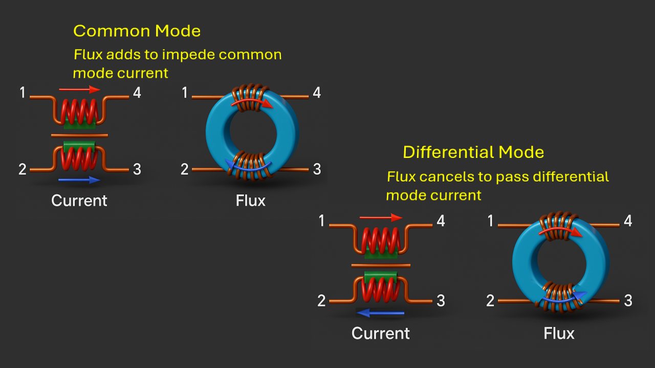
A common mode choke (CMC) is a type of passive filter made by winding two or more conductors (typically for a differential signal) on a magnetic core in such a way that:
Differential signals pass unaffected.
Common mode signals (noise present equally on both lines) induce magnetic flux in the same direction, which creates impedance and attenuates the noise.

Structure and Working Principle
A common mode choke is essentially a toroidal or cylindrical magnetic core (often ferrite or powdered iron) with two windings of wire wound around it—usually side by side or bifilar wound.
Key components:
- Magnetic Core:
- Typically ferrite material with high permeability.
- Acts as the medium for magnetic flux.
- Windings (Coils):
- Two insulated copper wires are wound around the core.
- The wires carry current for the differential signal (i.e., one wire for signal, one for return).
- Pins / Terminals:
- The choke is mounted on a PCB, with four pins—two for each coil end.
Working Principle of a Common Mode Choke
The common mode choke blocks common mode currents (noise or interference that flows in the same direction on both lines) but allows differential mode currents (normal signal current that flows in opposite directions) to pass freely.
Here’s how it works:
- For differential mode currents:
- Current flows in opposite directions in the two windings.
- Their magnetic fields cancel each other out in the core.
- Result: Minimal inductance → signal passes through with little impedance.
- For common mode currents (e.g., EMI or RF noise):
- Current flows in the same direction through both windings.
- Their magnetic fields add up, reinforcing the magnetic flux in the core.
- Result: High inductance → blocks or attenuates noise effectively.
Think of a CMC as a filter that says:
- "If the currents are opposite (real signal), I’ll let them through with no problem."
- "If the currents are the same (noise), I’ll choke them with high impedance."
Applications in PCB and System Design
Power lines: To suppress switching noise from DC-DC converters.
USB, HDMI, Ethernet: To block radiated and conducted emissions from high-speed I/O.
CAN/LIN buses: To reduce susceptibility and emissions in automotive networks.
Audio circuits: To remove hum and external noise from cables.
Design Considerations for Common Mode Chokes in EMI Suppression
Effective use of common mode chokes (CMCs) requires thoughtful integration into PCB and system-level designs. The following key design considerations ensure optimal EMI mitigation without compromising signal integrity or power delivery.
Common mode chokes (CMCs) are vital components in suppressing electromagnetic interference (EMI), particularly common mode noise that tends to couple onto cables and radiate from electronic systems. To achieve optimal performance, careful attention must be paid to several design factors that influence both EMI suppression and signal integrity.
1 Frequency Characteristics and Impedance Profile
The effectiveness of a CMC is highly dependent on its impedance profile across frequency. An ideal CMC offers high impedance to common mode noise while remaining transparent to differential mode signals. Design selection should be guided by the spectral content of the unwanted emissions. In most digital systems, common mode noise appears predominantly in the 10 MHz to 1 GHz range. Therefore, chokes must be selected based on insertion loss data provided by the manufacturer, ensuring that they provide sufficient attenuation in this band.
Example: In USB 2.0 applications, significant emissions occur between 30 MHz and 300 MHz. A CMC designed to provide high impedance within this band will help in meeting EMI compliance requirements such as CISPR 32 or FCC Part 15.
2 Current and Voltage Handling Capability
Another critical consideration is the current-carrying capability of the CMC. The selected choke must support the continuous operating current of the line without causing magnetic saturation of the core. Saturation significantly reduces the common mode impedance and thereby degrades EMI suppression performance. Additionally, the choke’s voltage rating must exceed the peak differential voltage on the line to prevent insulation failure or dielectric breakdown between windings.
3 Differential Mode Transparency
While the primary purpose of a CMC is to suppress common mode noise, it is equally important to ensure that differential mode signals are not attenuated or distorted. This is particularly relevant for high-speed data lines such as USB 3.0, HDMI, or Ethernet, where signal integrity is paramount. In such applications, low differential impedance and symmetrical winding structures are essential to minimize skew and avoid signal degradation.
4 Optimal Placement Strategy
The physical placement of the CMC on the PCB significantly impacts its effectiveness. It should be placed as close as possible to either the source of EMI (e.g., switching regulators) or the I/O connectors (e.g., USB or RJ45 jacks). This minimizes the path length through which common mode currents can radiate. In systems with well-defined subsystem boundaries, placing the choke at the interface helps isolate noise between domains.
5 PCB Layout Guidelines
Proper PCB layout is essential to maintain the effectiveness of the CMC. The traces connected to the choke must be routed symmetrically to preserve differential balance. Any mismatch can lead to mode conversion, wherein differential signals generate additional common mode noise. The loop area between the signal paths and their return currents should be minimized to reduce parasitic inductance. Moreover, ground stitching vias should be included near the choke to provide a low-impedance return path for high-frequency currents.
6 Core Material and Winding Structure
The core material plays a crucial role in determining the frequency response of the choke. Ferrite materials are widely used due to their high permeability and frequency-selective damping properties. The winding structure, especially bifilar winding, enhances common mode suppression by ensuring tight magnetic coupling while allowing differential signals to pass with minimal interference.
7 Thermal and Mechanical Considerations
As passive components, CMCs also dissipate heat due to core losses and copper resistance. Therefore, they should be selected with a current derating margin to account for ambient temperature, self-heating, and aging effects. The choice between surface-mount and through-hole packages depends on current requirements, thermal dissipation, and mechanical robustness. Surface-mount components are preferred for compact designs and automated assembly processes.
8 Multi-Channel and System-Level Integration
In systems with multiple parallel data lines (e.g., differential pairs in HDMI or Ethernet), multi-channel CMCs can reduce board space and ensure uniform filtering across all lines. However, inter-channel crosstalk and imbalance must be considered during layout and simulation. Additionally, CMCs should be included as part of a comprehensive EMI strategy, integrated with other filtering elements such as ferrite beads and LC filters.
9 EMC Compliance and Validation
Ultimately, the choice and integration of CMCs must be validated through EMI pre-compliance and compliance testing. Techniques such as Line Impedance Stabilization Network (LISN) measurements, spectrum analysis, and near-field probing help assess the effectiveness of common mode suppression. Iterative tuning of choke parameters and placement is often required to meet stringent regulatory limits.
Comparison with Other Filters
|
Filter Type |
Best For |
Blocks |
Notes |
|
Common Moe choke |
Common Mode EMI |
Common mode Noise |
Transparent to differential signals |
|
Ferrite Bead |
Broadband Suppression |
High Frequency Noise |
Acts as lossy inductors |
|
LC Filter |
Specific frequency range |
Both Common and differential Noise |
Requires careful tuning |
Example
Consider a USB 3.0 line:
Without a CMC: Common mode currents induced by fast switching can radiate via the cable, failing EMI tests.
With a CMC: Noise is attenuated before reaching the cable, ensuring compliance with standards like CISPR 32.
Automotive Pulses
Automotive pulses refer to specific transient voltage waveforms that occur in a vehicle's electrical system. These pulses are defined by standards (like ISO 7637, SAE J1113, or LV 124) and used primarily for EMC (Electromagnetic Compatibility) testing of automotive electronic components and systems.
These tests simulate real-world disturbances (like load dumps, switching transients, inductive kicks) to ensure components can survive and operate correctly in harsh automotive environments.
Modern vehicles contain many ECUs, sensors, and actuators. They're exposed to:
- Alternator spikes
- Battery disconnection
- Relay switching
- Ignition transients
- Electrostatic discharge (ESD)
To ensure reliable operation, these pulses are simulated and tested in labs.
Pulses as per ISO 7637-2
ISO 7637-2 (for 12V and 24V systems)
The most widely used for electrical transients on supply lines.
|
Pulse |
Description |
Typical Cause |
|
Pulse 1 |
Negative spike |
Battery disconnect while inductive loads are ON |
|
Pulse 2a/2b |
Positive/negative spikes |
Switching of inductive loads |
|
Pulse 3a/3b |
Fast transients |
Arising from relay contact bounce |
|
Pulse 4 |
Voltage drop |
Engine cranking |
|
Pulse 5 |
Load dump |
Battery disconnect while alternator is charging |
Pulse Characteristics (ISO 7637-2)
Pulse 1
- Negative Spike
- Cause: Battery disconnection from Inductive Loads (motor, Solenoid)
- Affect: Power supply circuit, Microcontroller

| Parameters | Nominal 12 V system | Nominal 24 V system |
| Us | −75 V to −150 V | −300 V to −600 V |
| Ri | 10 Ω | 50 Ω |
| td | 2 ms | 1 ms |
| tr | 1 μs | 3 μs |
| t1 | ≥0.5 s | |
| t2 | 200 ms | |
| t3 | <100 μs | |
Pulse 2a
- Positive Spike
- Cause: Sudden interruption of current due to sudden disconnection of large loads
- Affect: Voltage regulators and semiconductors devices

| Parameters | Nominal 12V & 24V system |
| Us | +37 V to +112 V |
| Ri | 2 Ω |
| td | 0.05 ms |
| tr | 1 μs |
| t1 | 0.2 s to 5 s |
Pulse 2b
- Negative Spike
- Cause: Alternator field decay, Alternator’s field winding de-energises after engine shutdown
- Affect: ECU Reset

| Parameters | Nominal 12 V system | Nominal 24 V system |
| Us | 10 V | 20 V |
| Ri | 0 Ω to 0.05 Ω | |
| td | 0.2 s to 2 s | |
| tr | 1 ms | |
| t12 | 1 ms | |
| t6 | 1 ms | |
Pulse 3a
- Fast Transients – Negative
- Cause: Relay chatter (very fast edge), switching processes. Characteristics of these transients are influenced by distributed capacitance and inductance of the wiring harness.
- Affect: Signal Interference and component malfunction

| Parameters | Nominal 12 V system | Nominal 24 V system |
| Us | −112 V to −220 V | −150 V to −300 V |
| Ri | 50 Ω | |
| td | 150 ns ± 45 ns | |
| tr | 5 ns ± 1.5 ns | |
| t1 | 100 μs | |
| t4 | 10 ms | |
| t5 | 90 ms | |
Pulse 3b
- Fast Transients – Positive
- Cause: Relay chatter (very fast edge), switching processes. Characteristics of these transients are influenced by distributed capacitance and inductance of the wiring harness.
- Affect: Sensors and controllers

| Parameters | Nominal 12 V system | Nominal 24 V system | |
| Us | +75 V to +150 V | +150 V to +300 V | |
| Ri | 50 Ω | ||
| td | 150 ns ± 45 ns | ||
| tr | 5 ns ± 1.5 ns | ||
| t1 | 100 μs | ||
| t4 | 10 ms | ||
| t5 | 90 ms | ||
Pulse 4
- Cranking Pulse - Slow Negative
- Cause: Supply voltage reduction caused by energising starter motor of internal combustion engine.
- Affect: Sensors and controllers

| Parameters | Nominal 12 V system | Nominal 24 V system |
| Us | − 6V to − 7V | − 12V to − 16V |
| Ua | − 2.5V to − 6V with |Ua| ≤ |Us| | − 5V to − 12V with |Ua| ≤ |Us| |
| Ri | 0 Ω to 0.02 Ω | |
| t7 | 15 ms to 40 ms | 50 ms to 100 ms |
| t8 | ≤ 50ms | |
| t9 | 0.5 s to 20 s | |
| t10 | 5ms | 10ms |
| t11 | 5ms to 100ms | 10ms to 100ms |
Pulse 5a – Load Dump
- Unsuppressed Alternator Surge- Without Protection
- In the event of a discharged battery being disconnected while the alternator is generating charging current and with other loads remaining on the alternator circuit at this moment.
- Affect: ECU, Sensor, Power circuit
| Parameters | Nominal 12 V system | Nominal 24 V system |
| Us | 65V to 87V | 123V to 174V |
| Ri | 0.5 Ω to 4 Ω | 1 Ω to 8 Ω |
| td | 40ms to 400ms | 100ms to 350ms |
| tr | 10ms | |
Pulse 5b – Load Dump
- Suppressed Alternator Surge- with protection (like Zener diode, TVS diode)
- In the event of a discharged battery being disconnected while the alternator is generating charging current and with other loads remaining on the alternator circuit at this moment.
- Affect: ECU, Sensor, Power circuit

| Parameters | Nominal 12 V system | Nominal 24 V system |
| Us | 65V to 87V | 123V to 174V |
| Us* | As specified by manufacturer | |
| td | 40ms to 400ms | 100ms to 350ms |
Testing Setup
Usually tested in the lab using an EMC test bench with:
- Pulse generators
- Coupling/decoupling networks
- Oscilloscopes
- Electronic loads or real DUTs
The DUT (Device Under Test) must withstand or operate normally depending on the pulse.
Other Standards
- SAE J1113 – Similar to ISO 7637, North American usage
- LV 124 / LV 148 – German standards for 12V/48V systems (used by BMW, VW, Daimler, etc.)
- ISO 16750-2 – Broader set including electrical load, jump start, reverse polarity, etc.